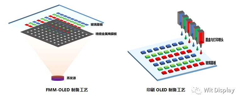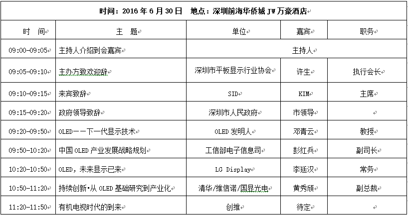


元器件交易網(wǎng)訊 4月2日消息,據(jù)外媒報(bào)道,日月光半導(dǎo)體公司(ASE)計(jì)劃與華亞科技聯(lián)合成立合資公司,該公司主要對器件使用3D封裝TSV(高密度的硅穿孔)技術(shù)。
ASE和華亞科已經(jīng)談判有一年多,并預(yù)計(jì)很快進(jìn)入進(jìn)程,該合資企業(yè)很可能被設(shè)置在華亞科技的閑置廠房或日月光工廠中。兩家公司最初的生產(chǎn)目標(biāo)是每月推出1萬片3D IC芯片,預(yù)計(jì)將擴(kuò)大TSV封裝范圍,包括應(yīng)用處理器和移動(dòng)RAM芯片。(元器件交易網(wǎng) 白玉濤譯)
以下為外文:
在ASE-華亞科合資公司也有可能與臺(tái)灣半導(dǎo)體制造公司(TSMC)在3D IC封裝業(yè)競爭,該消息人士指出。Advanced Semiconductor Engineering (ASE) reportedly plans to team up with Inotera Memories to set up a joint venture for handling TSV (through-silicon via) 3D IC packaging.
ASE and Inotera have been in talks for over a year and are expected to finalize the deal soon, said the sources, adding that the joint venture is likely to be set up either at a Inotera's idle plant or at a ASE plant in Chungli, north Taiwan.
Initial production aims are to roll out 10,000 3D IC chips a month, said the sources, adding that the two firms are expected to expand the TSV packaging technology to include application processors and mobile RAM chips.
The ASE-Inotera joint venture is also likely to compete with Taiwan Semiconductor Manufacturing Company (TSMC) in the 3D IC packaging sector, the sources noted.

關(guān)注我們

公眾號(hào):china_tp
微信名稱:亞威資訊
顯示行業(yè)頂級新媒體
掃一掃即可關(guān)注我們
產(chǎn)品供求| 雜志期刊| 協(xié)會(huì)服務(wù)| 專題集| 關(guān)于我們|網(wǎng)站地圖|版權(quán)聲明| 廣告服務(wù)
Copyright © 2018 深圳市美嘉投資有限公司. All Rights Reserved 版權(quán)所有 粵ICP備12048185號(hào)-1
中華顯示網(wǎng)所載文章、數(shù)據(jù)僅供參考,使用前務(wù)請仔細(xì)閱讀法律聲明,風(fēng)險(xiǎn)自負(fù)。


媒體合作:0755-86149081 廣告咨詢:0755-86149131 Email:314106127@qq.com